SMT printing fault analysis and solution
Surface Mount Technology (SMT) is one of the most popular technologies and processes in the electronics assembly industry today.It has the features of high assembly density, small size and light weight of electronic products.
Based on its fineness, a number of electronic products appear bad situation is caused by some problems in the production and processing of SMT processing.
Printing faults as a patch processing process is more common in the processing of a bad phenomenon, most of the electronic processing factory would like to find a way to improve the quality of their own SMD printing to solve and avoid printing faults. The following is an article about how we avoid print failures:
In order to reduce the failure rate, goson starts from the beginning with the BOM and Gerber data management, and strictly controls the procurement channels of components, storage and access control of solder paste, solder paste printing, SPI solder paste inspection, reflow soldering and other aspects.
According to statistics: 64% of the defects in the process of SMT mounting process comes from from incorrect solder paste printing. Therefore, to reduce the failure rate, to ensure the quality of PCBA products, we need to strictly control all aspects of SMT.
The following are several common SMT printing faults and solutions:
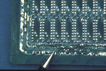
pull tip
Tip pulling: refers to the phenomenon of ‘small hills’ of solder paste on the pads after printing, which can easily lead to the scraper gap or the viscosity of the solder paste becomes larger.
Solution:
1. Clean or replace the stencil regularly;
2. Cleaning or replacing the PCB;
3. Adjusting printing parameters;
4. Replacement of better quality solder paste, thus reducing the generation of pull-tip.
5. Confirm whether the squeegee is worn and replace the squeegee (2. Type of squeegee:
6. There are two types of squeegee: plastic squeegee and steel squeegee. For ICs with a pitch of not more than 0.5mm, a steel squeegee should be used for printing to facilitate the forming of solder paste after printing).

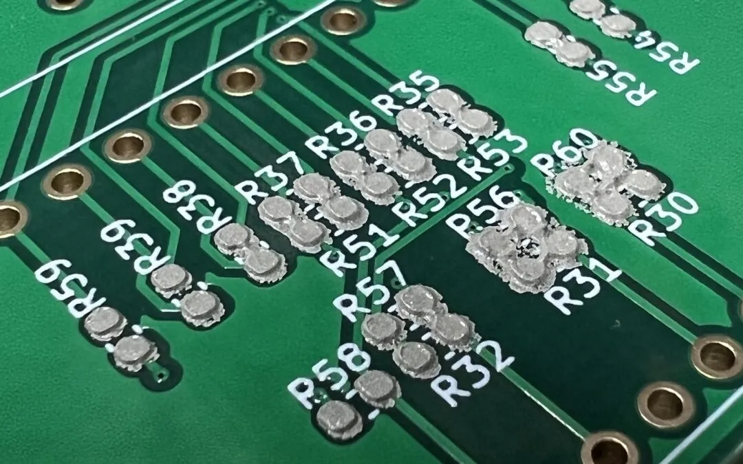
Inconsistent printing thickness
Thickness inconsistency: refers to the inconsistency of the thickness of the solder paste on the surface of the pad after printing, this type of phenomenon may be the cause of printing templates and PCBA circuit boards are not parallel, but also may be due to the particles of the solder paste is too large or uneven distribution of the impact of the squeegee work.
Solution:
1. Adjust the directions of the stencil to the circuit board
2. Select high quality solder paste for printing
Solder paste Slump
Solder paste Slump: refers to the printing of solder paste to both sides of the pad concave, generally caused by such phenomena are: squeegee pressure is too large, the PCB board being printed on the precise positioning of the instability of the viscosity of the solder paste or metal materials with low water content.
Solution:
1. Increase the proportion of metal components in solder paste; increase the viscosity of solder paste; reduce the particle size of tin powder;
2. Reducing the ambient temperature;
3. Reducing the thickness of the printed solder paste;
4. Enhancing the precision of the printed solder paste;
5. Adjusting the various construction parameters of the solder paste;
6. Reducing the pressure exerted by the placement of parts;
7. Avoid leaving the solder paste and the printed PCB in humid air for a long time;
8. Reducing the flux activity in the solder paste; reducing the lead content in the metal.
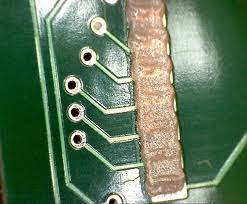
Raw edges or surfaces after printing
Raw Edge: It means that the printed circuit board has raw edges and is not smooth. If the viscosity of the solder paste is too low or the hole wall of the stencil opening is not smooth enough can cause this to happen.
Solution:
1. Select high quality solder paste
2. Check the smoothness of the hole wall when opening holes in the stencil