PCB inspection is the process of examining a printed circuit board (PCB) to ensure that it meets the required standards and specifications. The inspection process involves visually examining the PCB for defects, such as short circuits, open circuits, and incorrect component placement. It may also involve using specialised equipment, such as X-ray machines or automated optical inspection (AOI) systems, to detect hidden defects.
GOSON ensures the quality and reliability of electronic devices before delivery of PCBs.
We use several types of PCB inspections to detect and correct defects before equipment assembly, reducing the risk of failure and increasing customer satisfaction.
There are several types of PCB inspections, including:
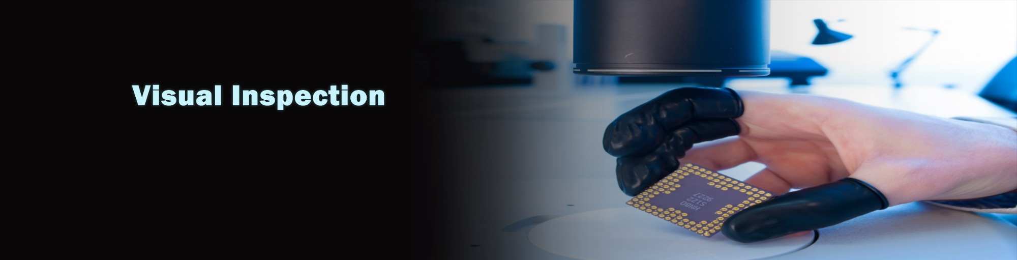
1.Visual Inspection
Visual inspection is a basic inspection method that examines the surface of a PCB by using the bare eye or a magnifying glass. This method can detect obvious defects such as poor soldering, missing or damaged components, and mislabelling. Although visual inspection is less efficient, it is still very effective in finding simple problems.
2.Automated Optical Inspection (AOI)
Automated Optical Inspection is a more advanced inspection method that uses a high-resolution camera and computer algorithms to automatically detect defects on the PCB.The AOI system quickly scans the entire PCB and identifies potential problems by comparing the actual image with an ideal image. This method is characterised by high speed and high accuracy and can greatly improve productivity.
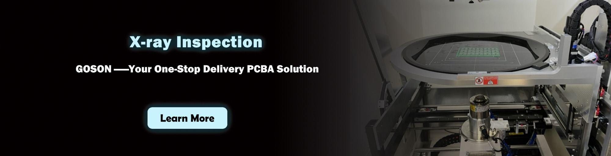
3.X-ray inspection
X-ray inspection is a non-destructive testing technique that can find defects that are not visible to the naked eye or AOI system, such as hidden components, internal cracks or bubbles. x-ray inspection can provide detailed information about the internal structure of the PCB, helping engineers to understand the potential problems and take appropriate measures to solve them.
4.Functional Testing
Functional testing is a testing methodology that verifies that a PCB functions as expected by simulating actual operating conditions. This method can detect potential problems in the design or manufacturing process and ensure that the PCB works properly before it is delivered to the customer. Functional testing usually requires specialised test equipment and test procedures to ensure the accuracy and reliability of the test results.
In short,GOSON through PCB Inspection, potential problems can be found and timely measures can be taken to solve them, so as to reduce product development and production costs and improve market competitiveness.
GOSON offers a full range of solutions for your circuit board production needs, including one-stop BOM matching services, electronic component sourcing and testing, manufacturing, testing/inspection and assembly.


