Designing your own printed circuit board (PCB) can be a challenging but rewarding process.
But at GOSON, we provide you with a ONE-STOP PCB design service, from preparing schematics to sourcing electronic components, to PCB fabrication and assembly, and finally to project delivery.GOSON is committed to providing you with PCB cost-containment services, fast delivery, and making your ideas a reality.
1ST STEPS - Determine the project requirements
1.Determine the project requirements
Determine the purpose of the printed circuit board and the features it needs to have. Consider factors such as board size, cost, and functionality
In determining the project requirements, it is first necessary to define the specific purpose of the printed circuit board (PCB), such as for communication equipment, medical equipment, automotive electronic systems, etc.. On this basis, the functions that the PCB needs to have, such as single-layer, double-layer, multi-layer, high-frequency, high-speed, high-density, etc., need to be further defined.
Next, the size of the circuit board needs to be fully considered, and the appropriate size needs to select based on the space constraints and installation requirements of the equipment. At the same time, the relationship between cost and functionality needs to be weighed to ensure that the PCB can meet the functional requirements while not exceeding the budget.
In addition, other factors of the PCB need to be considered, such as material, number of layers, impedance, vias, and soldering methods. These factors will directly affect the performance and reliability of the PCB, and therefore need to select according to the specific application environment and working conditions.
In short, when determining the project requirements, it is necessary to consider a variety of factors to ensure that the PCB can meet the performance needs and reliability requirements of the equipment.
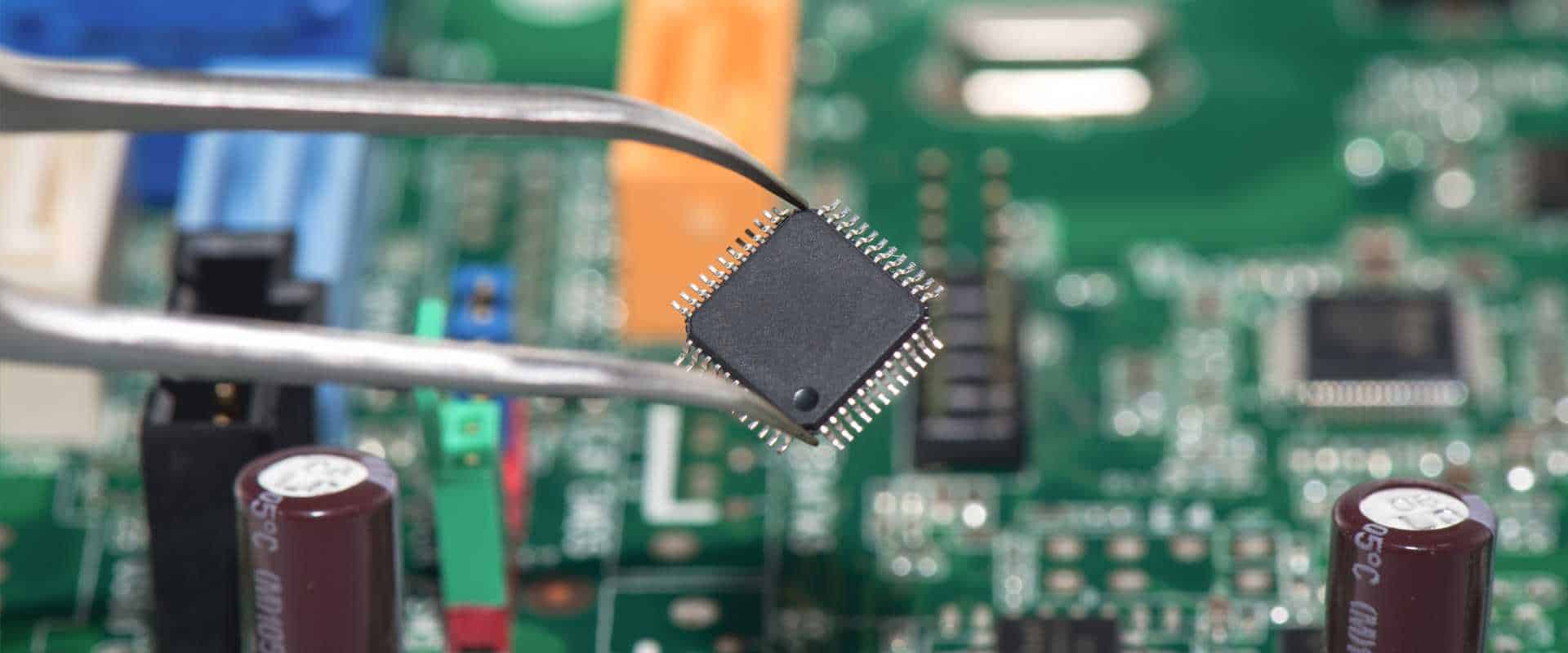
2.Select Components
Select the electronic components that will be used on the PCB, such as resistors, capacitors, and microcontrollers. Make sure that the components you select are compatible with each other and with the PCB design software you plan to use.
When selecting components, it is necessary to first determine the circuit function to be implemented on the PCB, and then select the appropriate electronic components according to the circuit function. Common electronic components include resistors, capacitors, inductors, transistors, microcontrollers, power supply modules and so on.
When selecting components, you need to pay attention to the following points:
1. Compatibility: Ensure that the select components are compatible with each other and will not cause problems such as electromagnetic interference or thermal effects. At the same time, it is also necessary to ensure that the components are compatible with the PCB design software to facilitate subsequent design and simulation.
2. Performance parameters: need to be based on the circuit's operating conditions and performance requirements, select components with appropriate performance parameters. For example, the choice of resistors need to consider its resistance, power, precision and other factors; the choice of capacitors need to consider its capacity, voltage, precision and other factors.
3. Package form: according to the size and layout of the PCB requirements, select the appropriate component package form. For example, the choice of SMD components or plug-in components, the choice of multi-pin package or single-pin package.
4. Reliability: Need to choose components with good reliability and stability to ensure the long-term stable operation of the PCB. You can refer to the certification standards and manufacturers of components such as the credibility of the choice.
In short, when selecting components, you need to consider the compatibility of components, performance parameters, package form and reliability and other factors to ensure the performance and reliability of the PCB.
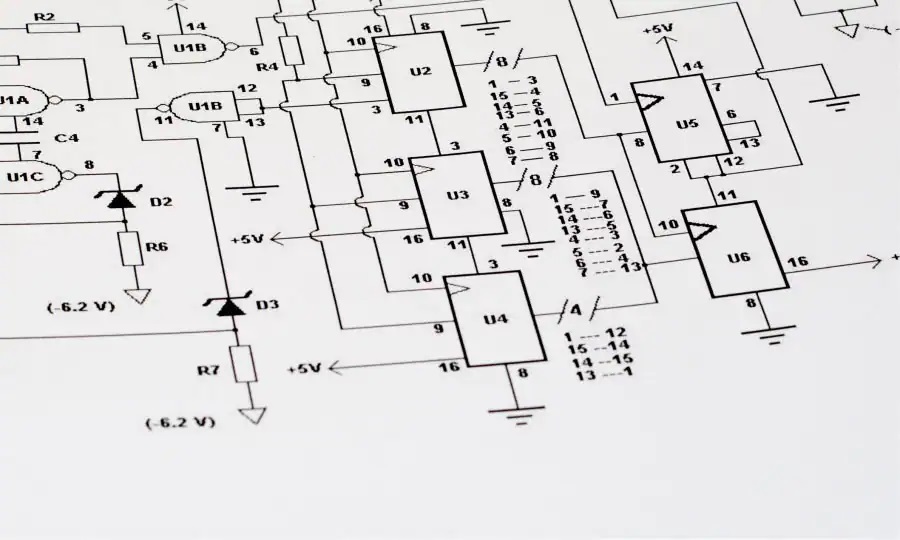
3.Create a circuit diagram
Using circuit design software, such as Eagle or KiCad, create a circuit diagram. The diagram should include a layout of all the components and their connections.
When creating circuit diagrams, you need to use professional circuit design software such as Eagle or KiCad. These software provide a rich library of components and design tools that can help designers quickly create circuit diagrams that meet the requirements.
When creating circuit diagrams, you need to follow the steps below:
1. Import component libraries: Import the required component libraries in the circuit design software, including resistors, capacitors, transistors, microcontrollers and other various electronic components.
2. Draw circuit diagrams: according to the circuit function and component layout requirements, draw circuit diagrams in the software. It should be noted that the circuit diagram should be clear and easy to understand, and the symbols and wiring of the components should comply with the electrical rules.
3. Configure component attributes: Configure the corresponding attributes for each component, such as component model, parameters, package form. This helps the subsequent PCB layout and simulation analysis.
4. Check and Modify: After completing the drawing of the circuit diagram, detailed checking and modification are required to ensure the correctness and completeness of the circuit diagram. You can use the checking tool in the software for automatic checking or manual checking.
5. Save and Export: Save the completed circuit diagram to a file and export it to the format required for PCB layout. Often, the circuit diagram and PCB layout need to be kept up-to-date to ensure design consistency.
In conclusion, when creating circuit diagrams, you need to be proficient in the operation of circuit design software, follow electrical rules and design specifications to ensure the correctness and completeness of circuit diagrams.
4.Create PCB Circuit Diagram
Using the same software, create a PCB circuit diagram that includes a layout of all components and their connections. Considerations include the size and shape of the board, the number of layers, and the routing of the wiring.
When creating PCB circuit diagrams, you need to use the same software that you use to create circuit diagrams, such as Eagle or KiCad. The following factors need to be considered when creating PCB circuit diagrams:
1. Size and shape of the circuit board: You need to select the appropriate size and shape of the circuit board according to the space constraints and installation requirements of the equipment. Also, the number of layers of the board, such as single, double or multi-layer, needs to be considered.
2. Wiring of the line: In the PCB circuit diagram, the wiring method and path of the line need to be considered. The wiring method can choose automatic wiring or manual wiring, according to the complexity of the circuit and personal preference. When wiring, you need to pay attention to the length of the line, the direction and spacing and other factors to ensure the stability and reliability of signal transmission.
3. Layout of components: In the PCB circuit diagram, it is necessary to consider the layout method and location of components. The layout of the components can choose the free layout or regular layout, according to the complexity of the circuit and personal preference. In the layout, you need to pay attention to the size, shape and pin number of components and other factors to ensure that the components can be soldered and maintainability.
4. Vias and pads: In PCB circuit diagrams, the size and location of vias and pads need to be considered. Vias are used to connect the lines between different layers and need to selecte according to the thickness of the line and the number of layers. Solder pads are used to connect components and lines, and need to select according to the package form of the component and the number of pins.
In short, when creating a PCB circuit diagram, you need to consider the size and shape of the board, the wiring of the lines, the layout of the components, the vias and pads, and other factors to ensure the performance and reliability of the PCB. It is also necessary to pay attention to the synchronous updating of circuit diagrams and PCB layouts to ensure the consistency of the design.
5.Review and test the design
Review the design carefully to ensure that it meets all the requirements of the project and that all components are connected correctly. You may also want to test the design by simulating or building a prototype.
When reviewing and testing a design, the entire design process needs to be carefully reviewed and tested to ensure that the design meets all the requirements of the project and that all components are connected correctly. The following are some of the steps involved in reviewing and testing a design:
1. Review Design Documentation: Review the design documentation, including circuit diagrams, PCB circuit diagrams, and design specifications to ensure that all design elements meet the project requirements and standards.
2. Simulation testing: Use circuit simulation software, such as LTspice or PSPICE, to perform simulation testing of the circuit. Through simulation testing, the performance and stability of the circuit can be verified and potential problems and defects can be found.
3. Prototyping: Create an actual prototype for practical testing and verification. Through prototype testing, the actual performance and reliability of the circuit can be verified, and problems and defects in the actual manufacturing and assembly can be found.
4. Testing and debugging: Detailed testing and debugging of the prototype to ensure that the performance and reliability of the circuit meets the requirements of the project. Testing and debugging includes electrical testing, functional testing and environmental testing.
5. Modification and improvement: According to the results of testing and debugging, the design is modified and improved to ensure the completeness and reliability of the design.
In conclusion, when reviewing and testing the design, the whole design process needs to be carefully reviewed and tested to ensure the integrity and reliability of the design. Potential problems and defects can be identified and the quality and reliability of the design can be improved through simulation testing and prototyping.
6.Fabricate and assemble the PCB
Once the design is complete, we will fabricate your PCBs.And after the PCB is fabricated, we will be able to place the components on the board for assembly.
In the process of making and assembling PCBs, the following steps need to be carried out:
In the process of making and assembling PCBs, the following steps need to be carried out:
1. Production of PCB: When the design is completed, the PCB circuit diagram needs to be sent to a professional PCB manufacturer for production. The manufacturer will make the PCB according to the circuit diagram, using photolithography, etching, copper plating, etc. In the process of making, you need to pay attention to the number of layers, size, material and other factors of the PCB to ensure the quality and performance of the PCB.
2. Select components: According to the circuit diagram, select suitable components, including resistors, capacitors, transistors, microcontrollers and so on. When selecting components, you need to consider the performance, package, price and other factors of the components.
3. Place components: Place the components on the PCB and connect each component according to the circuit diagram. When placing components, you need to pay attention to the direction, position, pin number and other factors to ensure the correctness and reliability of the components.
4. Soldering components: Use tools such as soldering iron or reflow soldering to solder the components on the PCB. During the soldering process, it is necessary to pay attention to factors such as soldering temperature, time and techniques to ensure the quality and reliability of the soldering.
5. Inspection and testing: After the assembly is completed, the PCB needs to be inspected and tested to ensure that the performance and reliability of the circuit meets the requirements of the project. Inspection and testing include electrical testing, functional testing and environmental testing.
6. Debugging and optimisation: If problems and defects are found during inspection and testing, debugging and optimisation are required. Debugging and optimisation include component replacement, line modification, parameter adjustment and so on.
In conclusion, in the process of making and assembling PCBs, factors such as PCB fabrication, component selection and placement, soldering, inspection and testing, debugging and optimisation need to be taken into account to ensure the quality and performance of the PCB.
In conclusion, in the process of making and assembling PCBs, factors such as PCB fabrication, component selection and placement, soldering, inspection and testing, debugging and optimisation need to be taken into account to ensure the quality and performance of the PCB.
GOSON offers a full range of solutions for your circuit board productin needs, including one-stop BOM matching services, electronic component sourcing and testing, manufacturing, testing/inspection and assembly.

20 years + industry experience meets your varied PCBA customisation needs
GOSON has over 5000 ㎡ of PCB manufacturing space and the world's most advanced production equipment ,which support the PCB surface processes: HASL-LFENlG, GOLD PLATED, TIN PLATED, SILVER PLATED, ENIPIG, OSP.
> 20+ Years industry experience
> 100+ Company employees
> 40% + Faster Design Cycles
> 1 Pieces + Lowest order quantity
> 190+ Customized solutions for clients


