Flexible PCB Capability
ABOUT Flexible PCB Capability
What is the Flexible Printed Circuit boards(Flexible PCB)
Printed Circuit Board Assembly, or simply PCBA, is the process of soldering electronic components onto a printed circuit board.

Flexible Printed Circuit Boards, also known as FPCBs(Or Flexibl PCBs), are made of flexible materials, such as polyimide film, which are highly flexible and have good solderability, making them widely used in applications that require these characteristics, such as smartphones, laptops and medical devices.

They are highly flexible and have good solderability, so they are widely used in applications that require these characteristics, such as smartphones, laptops and medical devices.

FPCBs are thinner and lighter than RPCBs and can be bent and twisted without damage. Therefore, they are used in applications where PCBs need to be moved or bent in a limited space.In addition, FPCBs offer better electrical performance and higher connection density, but are more expensive and difficult to manufacture than RPCBs.


GOSON expertise in Printed Circuit Board (PCB) mounting, electronic product design.We offer a full range of PCB products and services to help take your PCB project from conceptual design to successful completion.


Please send your PCB files and BOM list to info@gosonxm.com to get a quotation.
We would like to be your partner and waiting for your message.


PCBA usually includes the following steps:

1. Preparation: The first step in the PCBA process is the preparation phase, which includes obtaining the circuit board design and the necessary electronic components.
2. Component Sourcing: Once the board design has been obtained, the required electronic components need to be acquired. These components can be obtained from a variety of sources including manufacturers, distributors and online marketplaces.
3. Circuit Board Manufacturing: In this step, a printed circuit board will be created. This is usually done through etching, which involves applying chemicals to the board to remove areas that are not covered with copper traces.
4. Component Placement: Once the board has been created, the next step is to place the electronic components onto the board. This is usually done by automated machines that can accurately place the components in the specified locations on the board.
5. Soldering: After the components are placed, the next step is to solder them to the board. This is usually done through reflow soldering, a process that involves heating the components and the board to make them bond together.
6. Testing: The final step in the PCBA process is to test the assembled boards to ensure that they function properly. This can involve a variety of testing methods, including visual inspection, automated optical inspection and functional testing.

GOSON offers a full range of solutions for your circuit board production needs, including one-stop BOM matching services, electronic component sourcing and testing, manufacturing, testing/inspection and assembly.


20 years + industry experience meets your varied PCBA customisation needs

GOSON has over 5000 ㎡ of PCB manufacturing space and the world's most advanced production equipment ,which support the PCB surface processes: HASL-LFENlG, GOLD PLATED, TIN PLATED, SILVER PLATED, ENIPIG, OSP.

> 20+ Years industry experience

> 100+ Company employees

> 40% + Faster Design Cycles

> 1 Pieces + Lowest order quantity

> 190+ Customized solutions for clients
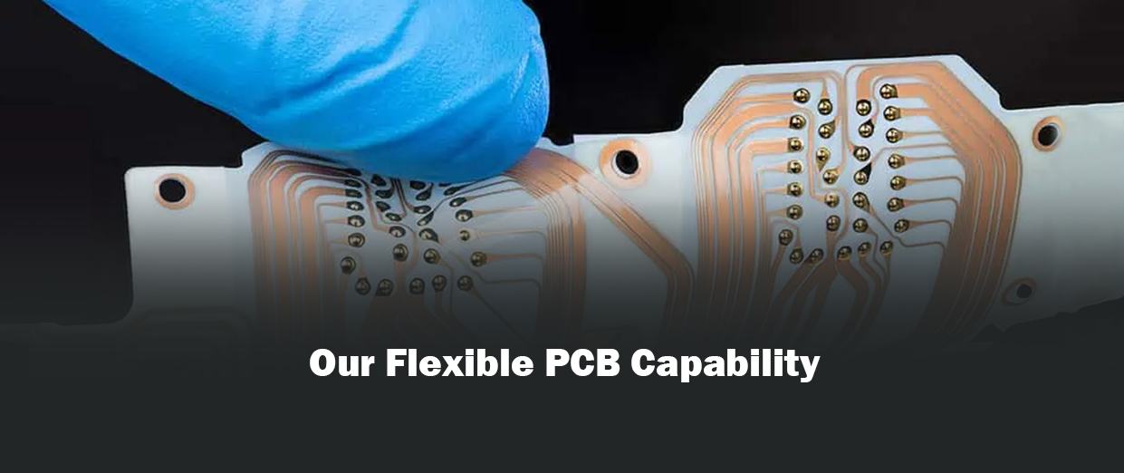


FPCB Specifications

Process Capability

Layer 1-12Layers
Maximum Board Thickness 0.05~2.5mm
Minimum Pitch 0.5mm
Minimum Alignment/Space
0.076mm

Copper to Board Edge

0.007"

Layer Openings

0.003"

Minimum Hole Diameter

8mil


Complete turnkey assembly 


Complete turnkey assembly including full service including:
 
● One-stop shopping for electronic components
Testing of components
Assembly of printed circuit boards
Quality control such as PCB board testing and functional testing
Order dispatch tracking and after sales service

Normal Procurement & Assembly Lead Times

The final lead time for PCB Assembly orders is the procurement lead time added to the assembly time.

Service

Times

Individual Assemblies 1-5 Working Days
Turnkey Assemblies
1-5 Working Days

On average, procurement time is typically 1-3 working days (based on the actual product).
Lead time for individual assemblies is 1-5 working days.s
Lead time for turnkey assemblies is 1-5 working days.

We provide you with a full range of turnkey services, providing you with one-stop supply delivery services, from BOM matching orders, engineer selection services, urgent orders, and even global search for your required hard-to-find item, coordinating the delivery time for you, solving the problem of component surplus, long delivery time, and saving your time and energy consumed in docking with multiple component suppliers and PCB factories.

GOSON is your PCB partner, able to fulfil your most complex requirements flexibly and reliably.
图x1:联系我们


Component Sourcing Lead Times


Contact our turnkey PCB assembly managers to get a proposal today.

Service

Times

ONE-STOP BOM Quote Service 0-2 Working Days
Component Soucing Time
2-5 Working Days(Based on the actual product)


pop_close
pop_main
Sign up for our newsletter
Get the most updated news and promotions first! Send us your urgent inquirement